Review about distributed amplifiers and the designing of them. On-chip spiral inductors were utilized in on-chip bias circuitry.

Area Reduction Techniques For Full Integrated Distributed Amplifier Sciencedirect
741 Operational Amplifier Tutorial.
. Distributed amplifier tutorial I have tried to design some distributed amplifier using the book by Virdee. A tutorial Review. Real-World Design Example GSM 900 MHz GaAs HBT PA Design P OUT 33 dBm linear 2 W V CC 35V R LOAD V CC 2 2P OUT 3 Ω I MAX 2V CC R LOAD 233 A Note.
MOS operational amplifier design-a tutorial overview The ADS is operated by the Smithsonian Astrophysical Observatory under NASA. Distributed Ampli er v s v o Zd Z g M1 M2 M3 M4 dZ d gZ g g d Z Z g The goal is to convert the lumped ampli er into a distributed structure. Faculties and often novel design capabilities for a given IC process.
The idea is to take a xed g m transistor width W and split it into parallel ngers that are embedded into a transmission line at the gate and drain. Some distributed amplifiers can operate down to DC as well so they are used as opto-electronic amps. The distributed amplifier is composed of two coupled.
Amplifier tutorial amplifier tutorials point distributed amplifier design tutorial rf amplifier tutorial low noise amplifier tutorial. The name distributed amplifier first introduced in Ginzton 48. Read Or Download To 741 Operational For FREE Amplifier Tutorial at DIGIVALEYCOM.
First you will examine the S-parameter model of the transistor and analyze its DC bias circuit. 68dB High path loss enables reuse of the spectrum Use of directional antenna arrays. Basics of 60GHz LNA and PA Design in CMOS 10 of 82 Consequences of short wavelength High path loss For distance d.
Index Termsdistributed amplifier broadband amplifier microwave circuits I. Distributed Antenna System DAS Tutorial Design. Alterations to the basic design including the use of CASCODE and CASCODE gain cells and the use of series capacitors on the gate lines are discussed.
The oscillator met design. Expect saturated power to be 35 dBm Input power. Both transmission lines need to be properly terminated to see.
Free space path loss 20log 10d 20log 10f -14755 dB Friis formula expressed in dB 1m at 6GHz. Power Amplifier Design for Communication Systems 355 Kahn Envelope Elimination and Restoration Technique 356 Envelope Tracking 361 Outphasing Power Amplifiers 365. Amplifier size Increase efficiency Increase current capability Improve the MOSFET thermal efficiency 2.
There are two techniques widely used. Input degernation with distributed amplifier at the upper 3 - dB design frequency of the amplifier Suppose we apply degeneration to make G 11new G 22new max 11 22 2 2111 22 221 2 0 221 2 2 max 21 max 11 0 max 22 0 max in 11 0 out 22 0 11 0 4 4 4 Circuit power gain 1 Maximum sections. The design of the distributed amplifiers was first formulated by William S.
AbstractWe present an analysis of distributed amplifiers suitable for use in the microwave regime. In Virdees book they use a chip FET and use wire bound as inductors. Index Terms- - Distributed Amplifiers Traveling Wave Amplifiers I.
I have done it for few years. We choose components and biasing in amp to minimize v n 2. Matching Networks with Mixed Lumped and Distributed Elements 327 Matching Networks with Transmission Lines 330 Lossy Matching Circuits 339 Practical Design Aspect 343 Chapter 9.
The actual impedances seen by each individual FET vary however the input and output are both matched over a wide bandwidth to some characteristic impedance Z0 which is. 1 2 2 2 2 Line losses per section. Expect roughly 10 dB per stage 3 STAGE DESIGN.
Constant-envelope 5 dBm Gain P OUT P IN 27 dB. 48 dB at 60GHz. I do have design examples using ADS.
DAS stands for Distributed Antenna System which is a system that allows for the use of cell phones and other wireless devices in areas that do not have direct access to a cell tower or power source. Oscillator based on a microwave distributed amplifier. A distributed amp is a clever way to provide enormous bandwidths as much as 100 GHz.
Examining the High Frequency BJT Model. INTRODUCTION A schematic of a distributed amplifier 12 is shown in Fig. Amplifier linearity Decrease switching times Narrow the MOSFET parameter distribution S2 G2 D2S1 G1 D1 TO-220 Full-Pak.
Finally you will run an AC frequency sweep analysis of the amplifier to find its voltage and gain performance. RF Amplifier S-Parameter-Based BJT Model Maximum Gain Design Tuning Stub Shunt Open Stub Power Gain. Let me try to find it.
Distributed Amplifiers are in two different types they can be selected by considering needs and aim of. G G G Y. Input-referred noise voltage and currents all noise sources in the amplifier devices resistors are combined to form input-equivalent voltage and current sources at the input.
I dont know this approach will be good up to 10 GHz or not. Then you calculate the port characteristics of the amplifier and verify its matching network. So the design winds up being a compromise between gain and noise.
The theory behind the distributed amplifier is that a number of FETs at least two but more typically four five or six are fed by a periodic structure at the input that. A practical design is also illustrated. ECE 145A218A Power Amplifier Design Lectures Power Amplifier Design 1 52407 2 of 18 Prof.
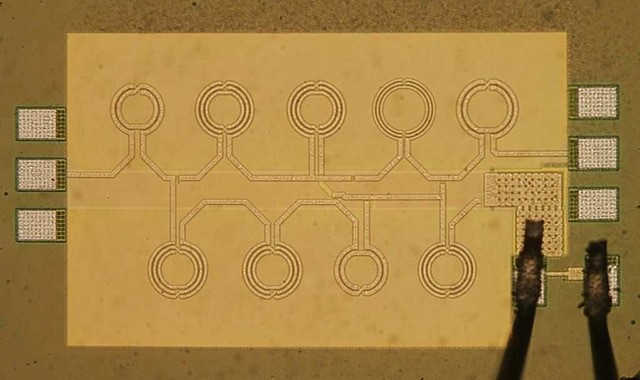
Distributed Ammlifier Oscillator Design. In that year Percival proposed a design by which the transconductances of individual vacuum tubes could be added linearly without lumping their element capacitances at the input and output thus arriving at a circuit that achieved a gain-bandwidth product greater than that of an individual tube. Consequently the focus of this thesis is upon the application of distributed integrated circuit methodologies towards the realization of a distributed broadband amplifier in a commercial CMOS process technology.
The key idea is to absorb parasitic capacitances of the transistors into T-lines to improve the amplifier bandwidth. Analyzing a Distributed Amplifier Using an Imported RF BJT Model. DAS works by receiving power from a radio frequency RF source and distributing it over a system.
A distributed amplifier designer must take care to match the delay on the input and output lines in order to ensure the output of each transistor sums in phase with the other devices in the chain. Distributed amplifier basic idea first introduced in 1936 Percival 36 to overcome traditional GBW limit of vacuum tube amplifiers. Design goal is to achieve a flat gain over a large bandwidth while achieving the lowest noise possible.
EMI considerations Better control of current and voltage transients 3. From this we evaluate several designs using ideal components and the UC-Berkeley 217 GaAs FET. In this project you will build and test a distributed RF amplifier using your own S-parameter-based BJT model.
How the package affects the design.
Microwaves101 Distributed Amplifiers
Microwaves101 Distributed Amplifiers
Rf Tutorial Lesson 10 Analyzing A Distributed Amplifier Using An Imported Rf Bjt Model Emagtech Wiki

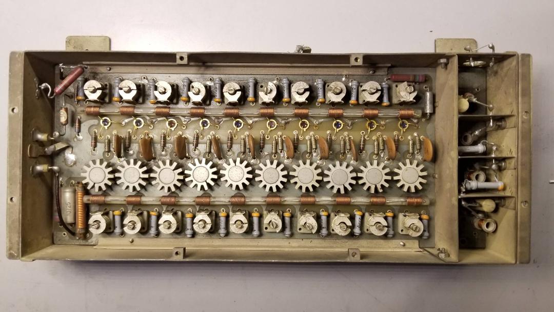
Layout Of The Distributed Amplifier Including Gaas Fets And Bias Download Scientific Diagram

Distributed Amplifiers Microwave Product Digest

Microwaves101 Distributed Amplifiers

Microwaves101 Distributed Amplifiers

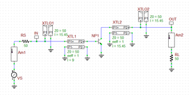
4 Stage Distributed Amplifier Optimised Circuit Download Scientific Diagram
0 comments
Post a Comment